

Introduction to DDR2
 2022-02-16 11:40:00
  722
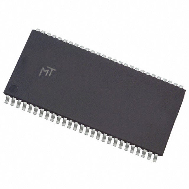
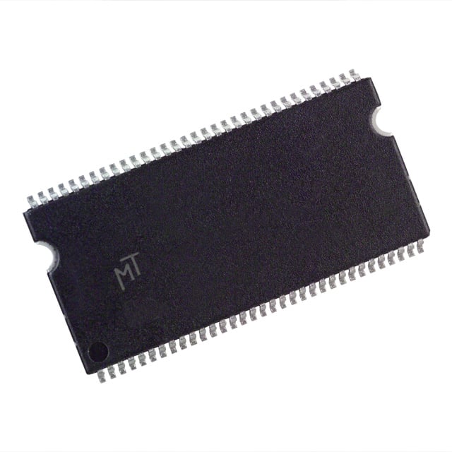
722DDR2 Synchronous Dynamic Random Access Memory (DDR2 SDRAM) is a double data rate (DDR) synchronous Dynamic Random Access Memory (SDRAM) interface. It replaced the original DDR SDRAM specification and itself was replaced by DDR3 SDRAM (introduced in 2007). DDR2 DIMMs are neither forward compatible with DDR3 nor backward DDR.
In addition to the double-pumping data bus in DDR SDRAM (transmitting data on the rising and falling edges of the bus clock signal), DDR2 allows higher bus speeds and reduces power consumption by running the internal clock at half the data bus speed. These two factors combine to produce a total of four data transfers per internal clock cycle.
Because the DDR2 internal clock runs at half the DDR external clock rate and DDR2 memory runs at the same external data bus clock rate as the DDR, DDR2 is able to provide the same bandwidth but with better latency. Alternatively, DDR2 memory running at twice the external data bus clock rate of DDR can provide twice the bandwidth and the same latency. The best rated DDR2 memory modules are at least twice as fast as the best DDR memory modules. Commercial DDR2 DIMMs have a maximum capacity of 8GB, but chipset support and availability for these DIMMs is minimal, and it is more common to use 2GB per DIMM.
DDR2 overview
The main difference between DDR2 and DDR SDRAM is the increase in prefetch length. In DDR SDRAM, the prefetch length is two digits of each word in each word; In DDR2 SDRAM, it is four bits. Four bits are read or written from a four-bit deep prefetch queue during access. The queue receives or transmits its data over the data bus over two data bus clock cycles (two bits per clock cycle). Increasing the prefetch length allows DDR2 SDRAM to double the rate at which data is transmitted over the data bus without correspondingly doubling the access rate of the DRAM array. DDR2 SDRAM is designed in this way to avoid excessive power consumption.
The bus frequency of DDR2 is improved by electrical interface improvements, on-chip termination, prefetch buffers, and off-chip drivers. However, as a trade-off, the latency increases significantly. The DDR2 prefetch buffer is 4 bits deep and DDR is 2 bits deep. While the typical read latency of DDR SDRAM is between 2 and 3 bus cycles, the read latency of DDR2 can be between 3 and 9 cycles, although the typical range is between 4 and 6. Therefore, DDR2 memory must run at twice the data rate to achieve the same latency.
Another cost of increasing bandwidth is to require the chip to come in a BGA package that is more expensive and difficult to assemble, compared to TSSOP packages such as DDR SDRAM and SDR SDRAM for previous generations of memory. This packaging change is necessary to maintain signal integrity at higher bus speeds.
The energy savings were achieved mainly due to the improvement of the manufacturing process through chip shrinkage, resulting in a drop in operating voltage (1.8 V compared to 2.5 V for DDR). Lower memory clock frequencies can also reduce power consumption in applications that do not require the highest available data rates.
According to JEDEC [4], the maximum recommended voltage is 1.9 volts, which should be considered an absolute maximum when memory stability is an issue, such as in servers or other mission-critical equipment. In addition, the JEDEC states that memory modules must withstand voltages up to 2.3 volts to cause permanent damage (although they may not actually work properly at that level).
Backward compatibility
DDR2 DIMMs are not backward compatible with DDR DIMMs. The notches on the DDR2 DIMMs are not located in the same position as the DDR DIMMs and have a higher pin density than DDR DIMMs in desktops. DDR2 is a 240-pin module and DDR is a 184-pin module. The notebook has 200-pin SO-DIMMs for DDR and DDR2; However, the grooves on the DDR2 module are slightly different from those on the DDR module.
High-speed DDR2 DIMMs can be mixed with low-speed DDR2 DIMMs, although the memory controller will run all DIMMs at the same speed as the current lowest-speed DIMMs.
Relationship to GDDR memory
GDDR2 is a form of GDDR SDRAM developed by Samsung and introduced in July 2002. [7] The first commercial product to claim to use "DDR9" technology was the Nvidia GeForce FX 2 graphics card. However, it is important to note that this GDDR5800 memory used on graphics cards is not DDR2 itself, but an early halfpoint between DDR and DDR2 technology. The use of "DDR2" to refer to GDDR2 is a colloquial misnomer. In particular, the double performance enhancement lacks I/O clock rate. It has serious overheating problems due to the nominal DDR voltage. ATI has since further designed GDDR technology into GDDR2, which is based on DDR3 SDRAM but adds some additional features for graphics cards.
GDDR3 and GDDR5 are now commonly used in modern graphics cards and some tablets. However, the budget and the appearance of mid-range graphics cards claiming to use "GDDR2" added further confusion. These cards actually use standard DDR2 chips and are designed to be used as main system memory, but run with higher latency to achieve higher clock rates. These chips cannot reach the clock frequency of GDDR3, but they are cheap and fast enough to be used as memory for mid-range graphics cards.
Related news